Skip to content
We are very optimistic about this place, so we have decided to move here for development. Looking at the park under construction, a person in charge of a contracted enterprise said with emotion.
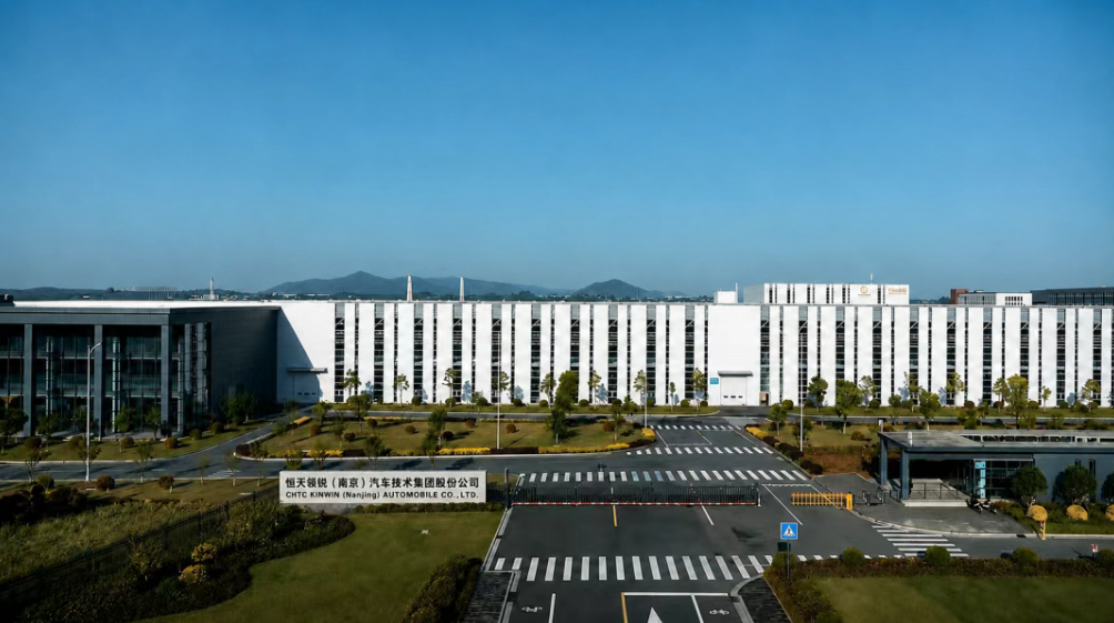
Recently, another major project in the new district has made new progress: the main structure of the second phase of the Optoelectronic Industrial park is about to be capped. It is worth mentioning that before the factory buildings are fully completed, the park has already been “fully signed up”, with several enterprises from the upstream and downstream of the photonic chip industry chain waiting to move in.
What does the park do?
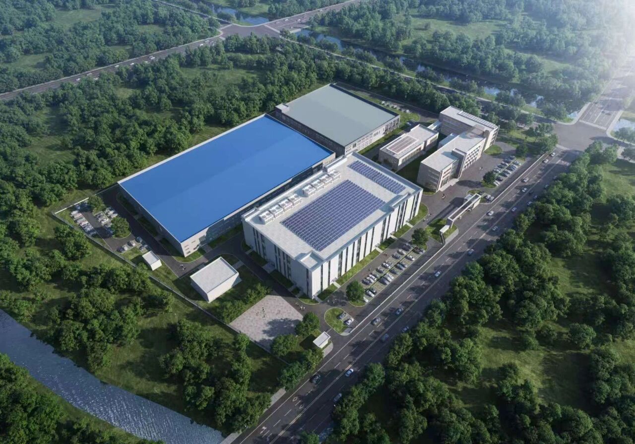
The second phase of the Optoelectronic Industrial Park project is located at No. 1, Yanxin Road, New District. Construction began at the end of February this year. Now, nearly 20,000 square meters of high-standard factory buildings have “risen from the ground”.
From the groundbreaking to the topping out, it took over 200 days, which was a little earlier than the original plan. The person in charge of the project construction party introduced.
So, what exactly is this park for? It is reported that at the very beginning of the planning, the project was positioned as a “pilot production and industrialization carrier zone for photonic chips”, tailored to the cutting-edge directions such as photonic chips, advanced materials, and high-end equipment.

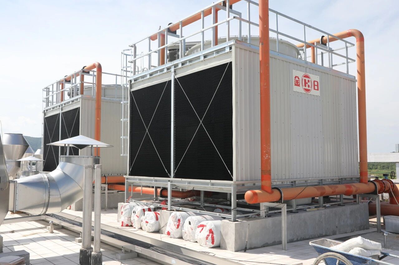
In the design of the factory building, the park determines the floor height, load and shock absorption schemes in combination with the requirements of the photoelectric process, and reserves professional Spaces such as clean rooms and chemical storage rooms. For instance, the first floor’s clear height of 7.9 meters, along with its reinforced load-bearing and anti-micro-vibration structure, is particularly suitable for the installation and stable operation of heavy precision equipment such as large-scale laser devices, photolithography machines, thin film etching, ion implantation, chemical vapor deposition, and physical vapor deposition.
On the other hand, in terms of functional layout, the second phase of the optoelectronic industrial park forms a “cluster” with the existing pilot production lines, research and development centers, and talent bases of the optoelectronic industry in the new district. Next to the second phase is Nanzhi Optoelectronics, a key optoelectronic public technology platform that the new district has focused on developing and building. It is also the first domestic enterprise capable of providing 8-inch thin-film lithium niobate tape-out services.
Such a layout enables seamless connection between research and development, pilot production and mass production. After the project is completed, it is expected to cover the entire chain of production and manufacturing of optoelectronic chips.
Which other enterprises are planning to settle in?
From the very beginning, by anchoring the track and clarifying the direction, project attraction will be more “accurate”. The second phase of the Optoelectronic industrial park is about to be topped out, and a number of high-quality projects have also been signed one after another and are waiting to move in.
Among them, there are both enterprises that have grown up in Jiangbei and innovative teams that have come from other cities in the Yangtze River Delta. They are all upstream and downstream enterprises in the photonic chip industry chain, covering fields such as design, manufacturing, packaging and testing. It is reported that after the enterprise is established, it is expected to drive the regional photonic chip industry to achieve a scale output value of 3 billion yuan.

“We almost inspected all the key parks across the country that are suitable for developing the photonic chip industry before deciding to settle down.” ” A person in charge of an optoelectronic chip enterprise from Suzhou said that the team not only needs to conduct pilot production but also take into account a certain scale of mass production, which has very high requirements for the site. The professional platforms and factories in the second phase of the optoelectronic industrial park are exactly what they need.
From the first contact to the confirmation of intention, the new district and the park have given us a very good impression – there are people to follow up on matters, solve problems and keep an eye on time. We didn’t simply rent a few floors; instead, we chose a place where we could take root and develop together for a long time. The person in charge sighed.
For local enterprises in Jiangbei, the sense of happiness of “a new production line growing right at their doorstep” is even stronger. Through the second phase of the Optoelectronic industrial park, the existing R&D and trial production lines of enterprises can be “perfectly connected” with the public process lines, testing centers and other platform resources of the park.
The new process will first undergo small-scale tests on public platforms and pilot lines, and then be introduced into production lines. When encountering process difficulties, please invite platform engineers and university teachers to come to the site for discussion together.” A business executive said, “If the park is responsible for coordinating the space, supporting facilities and elements well, we can focus on increasing production capacity.”
When the distance between production lines and process platforms is shortened from tens of kilometers to hundreds of meters, such industrial agglomeration will undoubtedly bring about a “leap” in efficiency, and the development of the industry will thus be injected with strong impetus.
Let’s look forward to the early commissioning of the second phase of the Optoelectronic industrial Park together